Ultimate Semiconductor Wafer Fabrication by Lesicopp
In the realm of cutting-edge technology, semiconductor wafer fabrication stands as a cornerstone, enabling the creation of the microchips that power our modern world. From smartphones to computers, automotive electronics to medical devices, semiconductor wafer fabrication plays a pivotal role in shaping our interconnected digital landscape. In this comprehensive guide, we delve deep into the intricate processes and technologies involved in semiconductor wafer fabrication, uncovering the fascinating journey of transforming raw materials into advanced semiconductor devices.
Understanding Semiconductor Wafer Fabrication:
Semiconductor wafer fabrication, also known as semiconductor manufacturing or semiconductor processing, encompasses a series of highly sophisticated processes aimed at creating integrated circuits (ICs) on semiconductor wafers. These wafers, typically made of silicon, serve as the foundation for building microchips with intricate circuitry.
The Fabrication Process:
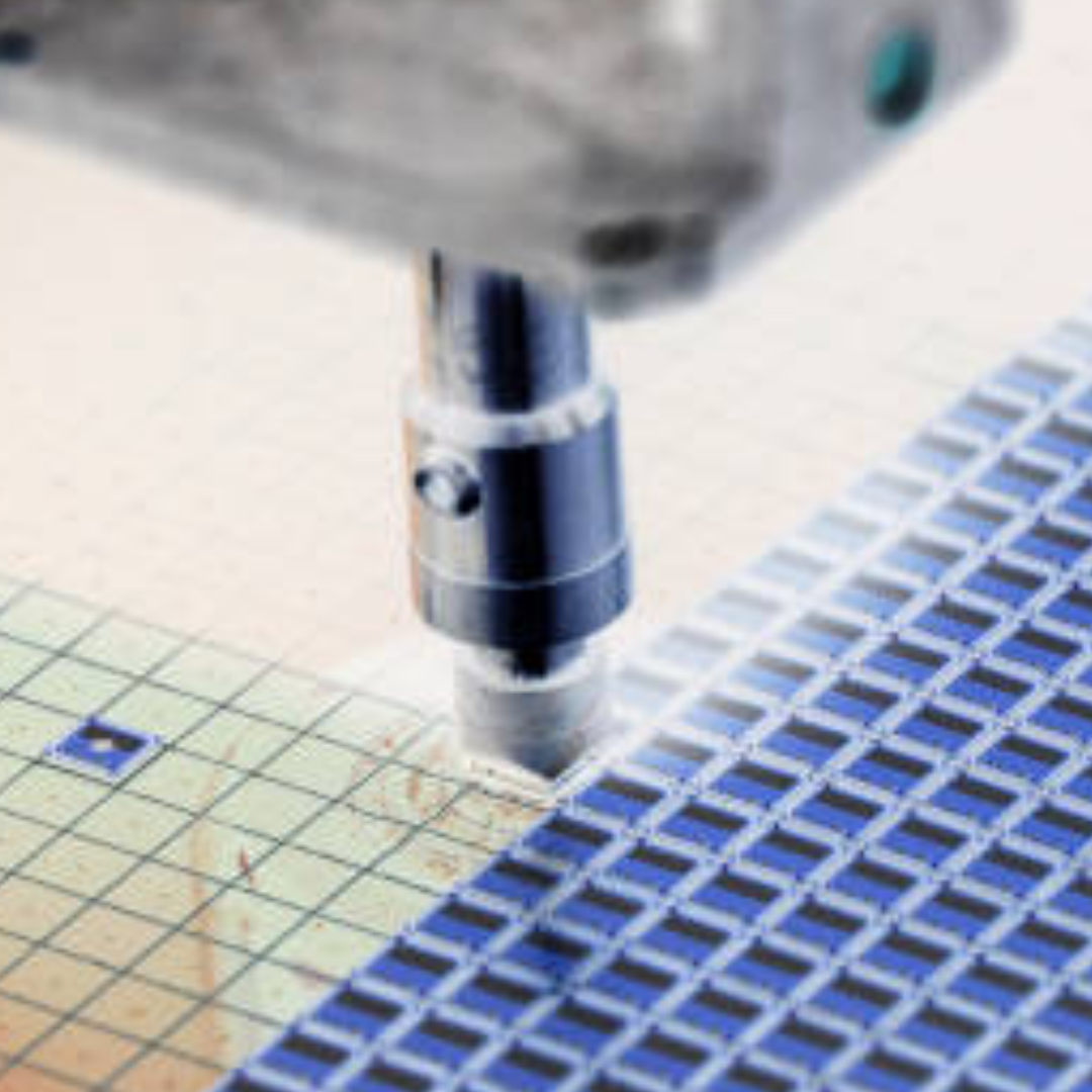
Wafer Preparation:
The process begins with the selection of high-purity silicon wafers, which undergo thorough cleaning and polishing to remove impurities and imperfections. A thin layer of silicon dioxide (SiO2) is deposited on the wafer surface through techniques like thermal oxidation or chemical vapor deposition (CVD). This oxide layer acts as an insulator and helps in subsequent steps of the fabrication process.
Photolithography: Photolithography is a crucial step where the desired circuit patterns are transferred onto the wafer. This involves coating the wafer with a light-sensitive photoresist material. A photomask, containing the pattern of the circuit design, is placed over the wafer, and ultraviolet (UV) light is used to expose the photoresist, creating the pattern on the wafer surface.
Etching: Etching is used to selectively remove material from the wafer according to the pattern created in the previous step. This can be done through wet etching using chemical solutions or dry etching using plasma. The etching process defines the circuit features such as transistors, interconnects, and contact points on the wafer.
Doping: Doping involves introducing impurities into specific regions of the silicon wafer to modify its electrical properties. This is achieved by depositing dopant materials such as phosphorus or boron onto the wafer surface. The dopants alter the conductivity of the silicon, creating regions with desired electrical characteristics like n-type (negative) or p-type (positive) conductivity.
Deposition: Thin film deposition techniques like physical vapor deposition (PVD) or chemical vapor deposition (CVD) are used to add layers of materials such as metals (e.g., aluminum, copper) or insulators (e.g., silicon dioxide, silicon nitride) onto the wafer. These deposited layers form the components of the integrated circuit, including metal interconnects, insulating layers, and transistor gates.
Annealing: Annealing is a heat treatment process used to activate dopants, repair crystal defects, and improve the overall electrical performance of the fabricated devices. This step involves subjecting the wafer to controlled temperatures in specialized furnaces.
Packaging and Testing: After the fabrication process is complete, individual semiconductor chips are separated from the wafer through dicing. These chips undergo packaging, where they are enclosed in protective casings and connected to external leads. Rigorous testing procedures, including electrical testing and functional testing, ensure the quality and functionality of the fabricated semiconductor devices before they are ready for commercial use.
Emerging Trends and Innovations:
The field of semiconductor wafer fabrication is constantly evolving, driven by advancements in materials science, nanotechnology, and manufacturing techniques. Some notable trends and innovations shaping the industry include:
Extreme Ultraviolet Lithography (EUV): EUV lithography is a next-generation technology that enables the creation of finer and more complex circuit patterns, leading to higher-performance microchips with reduced energy consumption.
3D Integration: This approach involves stacking multiple layers of semiconductor devices on top of each other, increasing device density and enhancing performance while minimizing footprint.
Advanced Materials: The exploration of novel materials such as gallium nitride (GaN) and silicon carbide (SiC) is enabling the development of power-efficient and high-frequency semiconductor devices for applications in power electronics and wireless communications.
Internet of Things (IoT) Integration: Semiconductor manufacturers are focusing on producing specialized chips optimized for IoT devices, facilitating seamless connectivity and data processing in smart systems.
Conclusion:
Semiconductor wafer fabrication is a complex yet indispensable process that underpins the advancement of modern technology. From the intricacies of photolithography to the precision of doping and deposition, each step in the fabrication journey contributes to the creation of high-performance semiconductor devices. As the industry continues to innovate and push the boundaries of what’s possible, semiconductor wafer fabrication remains at the forefront of technological progress, driving innovation across diverse sectors and shaping the future of digital transformation.